Printed Circuit Board Assembly?
Circuit Board Assembly
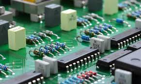
Printed circuit boards (PCBs) are used in the construction of electronic devices and electrical products. The conductive pathways engraved in the laminated copper sheets of PCBs provide the necessary connection between various electrical components. In assembly, the bare PCB is populated or “stuffed” with electronic components to form a functional circuit board, also known as a printed circuit board assembly (PCBA).
The simplest PCBs are single-sided. However, two-sided PCBs are more common, and require different fabrication processes. PCBAs are assembled with either through-hole or surface mount technology. Traditionally, through-hole construction was the preferred method for circuit board assembly. Component leads were inserted through holes in the PCB and soldered to the copper PCB traces. This process required a large number of hand tools and was slow, but allowed for high component densities. With the development of new etching and lamination technologies, this process was improved significantly.
A new method of assembling PCBs was introduced in the 1960s, called surface-mount technology. Using this method, components were placed on the surface of the PCBs so their pins lined up with the conductive pads or lands on the surfaces of the PCBs. Solder paste was then applied to these pads or lands, and the components were placed on top of the paste. The PCBs were then heated to a temperature known as the reflow zone, which melts the solder. The melted solder then bonds to the pad or land, holding the component in place.
Printed Circuit Board Assembly?
With the advent of SMT technology, it became possible to build much more complex and smaller electronic products. These products are now commonly found in consumer electronics, office equipment, and many industrial devices. This method of assembly is also faster than through-hole and requires less manual labor, allowing for greater production rates.
One issue that arose with SMT is the possibility of shorts between adjacent components. This is a result of movement of the components during the reflow process, which can cause them to connect with portions of the circuit that shouldn’t be connected. To reduce this problem, SMT manufacturing typically uses stencils and reflow zones for each side of the PCB. During the reflow process, the side of the PCB with the fewer and smaller surface mount components is first stenciled and placed, then reflowed. This ensures that the components stay put until the other side of the PCB is stenciled, placed and reflowed as well.
After all the component placement and soldering steps are complete, the PCBs are inspected for functionality. This step is critical to ensure that the assembly has achieved its intended function. Power and simulated signals are run through the circuit board, while testers monitor its electrical characteristics. If the PCB fails to function as designed, it is rejected for rework or scrap.
Despite their usefulness, PCBs are often static sensitive and need to be handled with care. They must be stored in antistatic bags and, if handled manually, the workers handling them should be grounded or otherwise prevented from picking up an electrostatic charge that might damage the components.